Recent advancements in the field of physics have ushered in a new class of materials with exceptional superconducting and metallic properties, as demonstrated by a team of physicists from MIT and their collaborators. In their study, published in the prestigious journal Nature, the researchers outline the creation of a novel material characterized by its unique wavy atomic layers, which measure only billionths of a meter in thickness. The innovative synthesis of this material not only allows it to be manipulated in macroscopic forms but also provides a more accessible means to explore its quantum behaviors.
The Unique Properties of Wavy Layer Structures
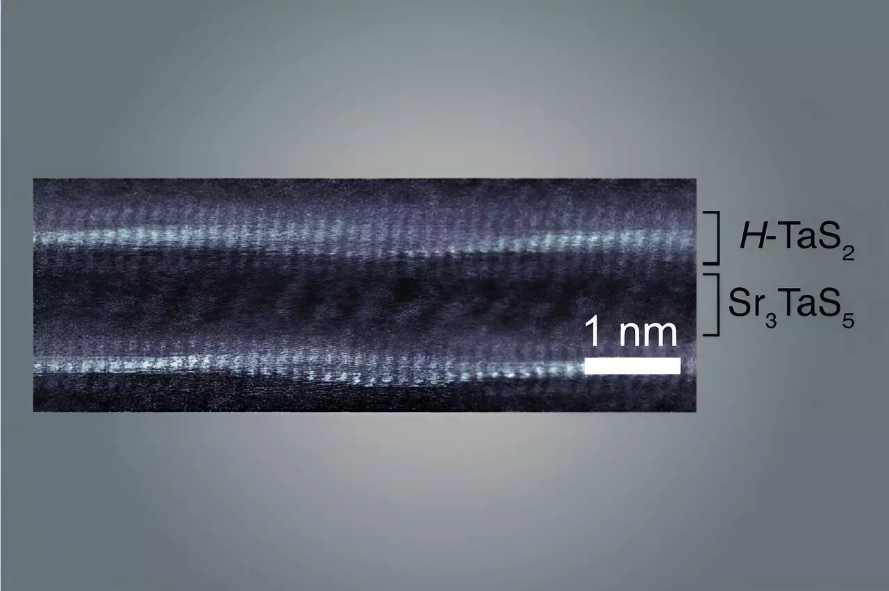
One of the most remarkable features of this new material is its composition, which includes alternating layers of tantalum and sulfur, alongside a spacer layer made of strontium, tantalum, and sulfur. This layered architecture causes the atomic arrangement within the material to adopt a wavy structure, resulting from the size discrepancies between different layers’ crystal lattices. This intrinsic design is more than just aesthetically intriguing; it significantly influences the material’s superconducting capabilities. At specific temperatures, the material demonstrates superconductivity, a state wherein electrons traverse effortlessly through the material without resistance—a phenomenon critical for developing advanced electronic devices.
Joseph Checkelsky, a senior investigator and Associate Professor of Physics at MIT, emphasizes the excitement surrounding these materials, stating they transcend traditional notions of crystalline structures. As researchers venture into the properties emerging from these unconventional designs, the opportunity for new scientific discoveries becomes practically limitless.
The synthesis of this wavy material involves a rational design approach, predicated on an in-depth understanding of materials science and chemistry. Unlike existing materials that exhibit wavy atomic structures, this new creation represents a methodological breakthrough, as it can be produced on a larger scale. Previous moiré materials required intricate manual assembly, making them less practical for experimental exploration. In contrast, the MIT team’s method involves combining powders in a furnace at elevated temperatures, where natural chemical reactions occur, eventually yielding uniform and sizable crystals conducive to detailed study.
Aravind Devarakonda, a Ph.D. graduate from MIT and the first author of the Nature paper, praises this innovative approach, remarking on how it elevates the feasibility of developing materials with unique properties. By leveraging the principles of chemistry and atomic interactions, this technique opens doors to a multitude of potential new materials yet to be discovered.
From a physical perspective, the formation of the wavy layers within the new material emerges from the structural misalignment between the layers. This issue creates a phenomenon similar to spilling over a stack of legal-sized paper over standard-sized paper—leading to a buckling effect essential for the development of the wavy characteristics. The significance of this design shouldn’t be understated, as it directly contributes to the intriguing behaviors exhibited by the material.
The presence of these structural modulations influences the superconductivity of the electrons; their movement is intricately linked to the wave-like configuration. In some regions, superconductivity appears enhanced, while it diminishes in others, indicating a unique relationship between the material’s microstructure and its macroscopic properties.
As this research continues to evolve, the ability to manipulate the newly discovered materials unlocks a world of possibilities in technology and materials science. The capacity to engineer materials with tailored electronic properties could revolutionize the development of sophisticated electronic devices, quantum computing, and energy-efficient technologies.
The newfound ease in material synthesis and manipulation offers a promising avenue for researchers. Checkelsky and Devarakonda envision future studies that could yield even more remarkable materials through continued exploration of this family of compounds. With each revelation, scientists not only deepen their understanding of fundamental physics but also create the potential for innovative applications that could have a profound impact on various fields, from computing to renewable energy technologies.
This discovery of wavy atomic materials represents a significant milestone in the field of condensed matter physics. The work by MIT physicists highlights the impact of innovative approaches in materials synthesis, bridging the gap between theoretical insights and practical applications. As researchers continue to explore the untapped potential of these materials, one can only anticipate the extraordinary technologies and scientific revelations that will emerge from this uncharted territory.