Recent advancements in semiconductor research have reached a pivotal moment with UC Santa Barbara’s groundbreaking achievement in visualizing electric charge movements at the interface of different semiconductor materials. Utilizing the innovative scanning ultrafast electron microscopy (SUEM) techniques crafted by the Bolin Liao lab, researchers have unveiled the transient behavior of photocarriers for the first time. With insights drawn from this research, the broader implications on semiconductor theory, engineering applications, and energy efficiency are becoming increasingly apparent.
Photocarriers are intrinsic to modern electronic devices, particularly solar cells, where sunlight generates pairs of electrons and holes within a semiconductor layer. When photons energize these semiconductors, they create a flow of electric current as electrons move and separate from their corresponding holes. This process holds monumental potential; however, traditionally, much of the energy from these excited states dissipates in mere picoseconds, resulting in a meager amount of usable energy in standard photovoltaic systems. By understanding how these hot carriers behave before they lose their energy, researchers can push the boundaries of energy efficiency and improve device performance.
The transient nature of hot carriers poses challenges and opportunities. Despite indirect measurements providing some insights, the ability to directly visualize this phenomenon is crucial for semiconductor materials science. Bolin Liao articulated this significance succinctly, noting that many theories exist without direct empirical support. By showcasing these processes visually, researchers can establish benchmarks to validate or challenge existing theories.
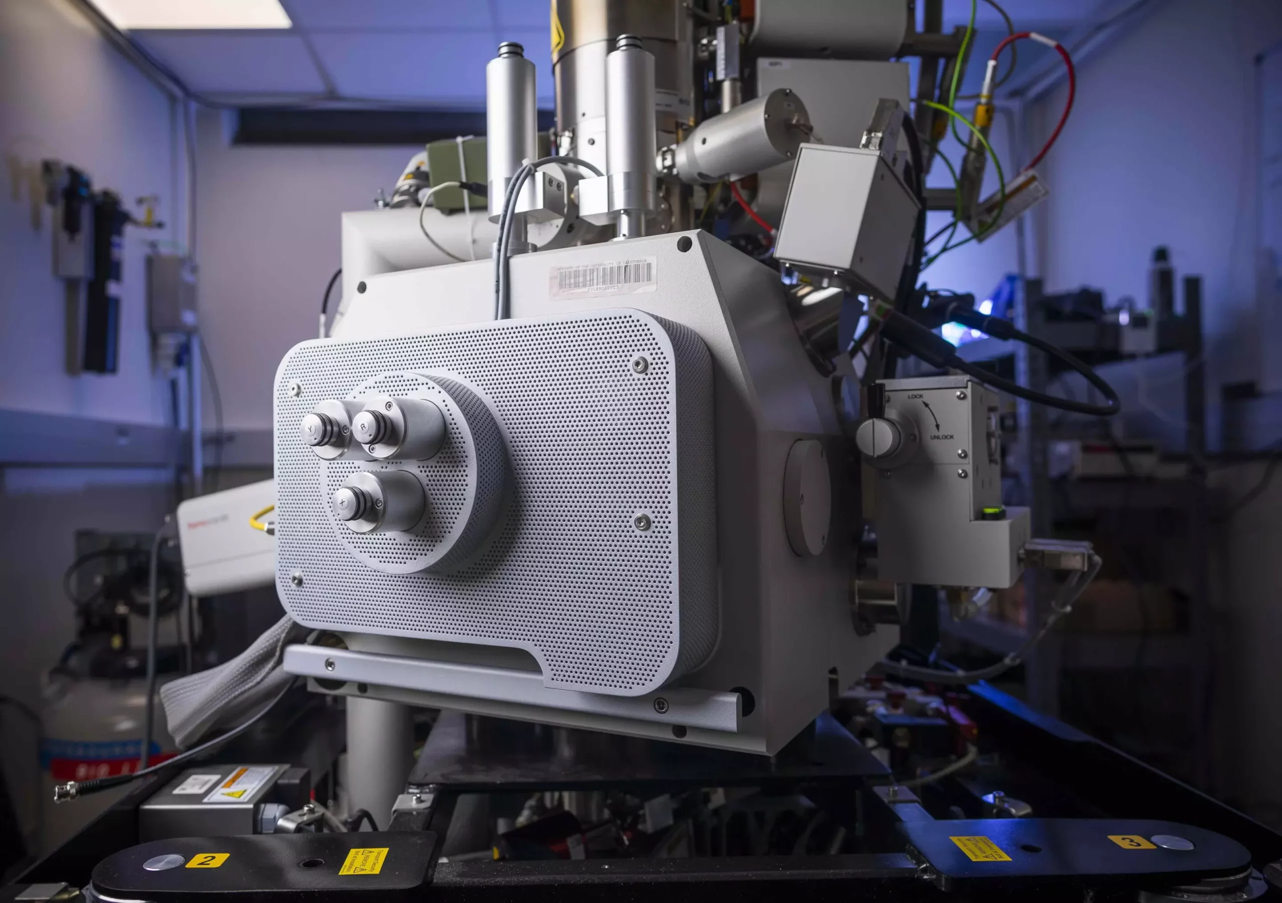
The experimental setup utilized by Liao’s team employed ultrafast laser pulses as a mechanism akin to a shutter, capturing the fleeting behavior of hot carriers. This innovative methodology allows researchers to ‘film’ events at an unprecedented time resolution, thus providing insights into the rapid movements occurring on the picosecond to nanosecond scale. The researchers focused their attention on a silicon-germanium heterojunction, a junction that could significantly impact fields such as photovoltaics and telecommunications.
One of the key revelations from this work pertains to the behavior of hot carriers as they traverse these heterojunctions. With the initial high temperature offering rapid speeds within the semiconductor, the scenario changes close to the junction interface where a portion of these carriers encounter trapping potentials, slowing their mobility. This phenomenon illustrates the complexity of carrier behavior in solid-state physics and highlights a critical challenge for device design.
The phenomenon of charge trapping within Si/Ge heterojunctions underscores the pivotal role interfaces play in semiconductor behavior. While theoretical frameworks exist to describe this, the direct visualization has unveiled a concrete understanding of how these mechanisms function. The ability to witness this intriguing dynamic allows for a more nuanced approach to semiconductor device design, steering efforts toward mitigating issues that arise from trapped charges, which in turn could enhance device efficiency.
Liao notes the unexpected nature of their findings, reinforcing that even established theories can benefit from experimental validation. This makes the clear observation of charge trapping crucial. It serves as both a lesson for ongoing research and a guide for improving existing technology, suggesting a pathway where design solutions can be influenced by empirical data.
The current research catalyzes a full-circle moment in semiconductor studies at UC Santa Barbara, linking present advancements back to the foundational ideas introduced by the late Herb Kroemer. Standing as a pioneer in semiconductor heterostructures, he asserted that the interface itself could serve as a functional device element. His visionary perspectives have paved the way for contemporary understanding of microelectronics, solidifying the importance of interface dynamics in modern devices ranging from computers to communication systems.
The successful demonstration of this novel imaging technique invites optimism for future applications in semiconductor research. Innovations in areas such as energy capture, sensor technology, and electronic devices stand to benefit immensely from this newfound capability. Direct observation of phenomena previously relegated to theoretical discourse empowers researchers to challenge existing notions while exploring potential avenues for improvement.
The visualization of charge carrier dynamics not only heightens interest in semiconductor materials but also emphasizes a more holistic approach to device engineering. These insights may inspire a new wave of technologies that harness the full potential of hot photocarriers, driving advancements that align with global energy efficiency goals.
The achievements of UC Santa Barbara’s team in visualizing hot carrier dynamics signify not just a technical milestone but a potential paradigm shift in the semiconductor landscape. As research continues to evolve, so too does the understanding of these materials, providing invaluable insights into one of the cornerstones of modern technology.