In the ever-evolving landscape of technology, optical materials play a pivotal role across a multitude of sectors, including telecommunications, healthcare, and consumer electronics. These materials are essential for various applications, such as industrial sensors and Organic Light-Emitting Diodes (OLEDs), where the management of light reflection and absorption is vital. However, one of the most significant challenges facing the industry is the prohibitively high cost associated with the production and quality control of these materials. Due to complex manufacturing processes and reliance on rare and expensive materials, the sustainability of optical materials has come into question. Recent research from esteemed scientists in Japan, notably Professor Hiroshi Moriwaki and Associate Professor Shouhei Koyama from Shinshu University, proposes a groundbreaking alternative that could shift the paradigm in this field.
The innovative study published in “Optical Materials” highlights how plasma—an electrically charged gas—can be harnessed to modify the optical properties of an accessible and inexpensive material: pencil lead. The researchers explored how to manipulate the reflectance properties of pencil lead samples through plasma irradiation, a method that promises to make optical materials more affordable and easier to produce. The technique effectively alters the surface by using plasma to etch away graphite, revealing the clay underneath, which acts as a thin layer that contributes to light interference effects.
The transformational process begins with pencil lead, a ubiquitous and low-cost material that has long been overlooked in high-tech applications. By studying the interaction between clay and graphite within pencil lead, the researchers have stumbled upon a method that allows for the creation of “structural colors.” This effect is not simply aesthetic; it results from the phenomenon of thin-layer interference, which can be precisely tuned through the duration of plasma exposure. In their method, lead samples undergo plasma irradiation for variable time intervals, revealing not only visible light modifications but also profound effects in the near-infrared and mid-infrared spectra.
The researchers’ systematic approach included analyzing how the duration and intensity of plasma exposure altered the optical characteristics of the lead samples. They discovered that extended treatments yield greater clay thickness, improving light interference effects, creating materials with intriguing potential applications. This methodological exploration is not just a technical achievement; it symbolizes a shift towards resource-efficient optical materials.
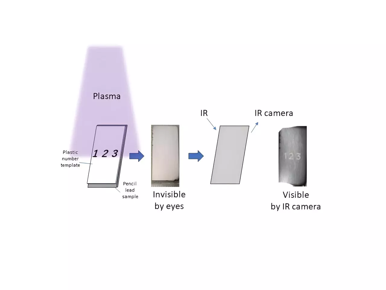
Among the significant breakthroughs reported by the research team is the ability to etch invisible characters onto the surface of pencil lead. When viewed through an infrared camera, these markings become visible, illuminating the potential for security applications in anti-counterfeiting technologies and watermarking. Such developments hint at a future where accessible materials can contribute to security innovations in an environmentally sustainable manner, expanding the horizons of how we use everyday items.
Prof. Moriwaki’s vision extends beyond the laboratory; he foresees applications that may lead to the creation of new printing technologies, where the same principles could be integrated into commercial products. Imagine a world where every printer uses pencil lead-based compounds, creating documents that are not only clear to the naked eye but also embedded with hidden information that is only accessible via special equipment.
The implications of this research are profound. The ability to utilize a common material like pencil lead to produce optical substances with reduced manufacturing costs presents a compelling case for redefining how such materials are sourced and produced. Given the existing economic and environmental pressures in the production of optical materials—rooted largely in the use of rare earth elements—the innovative approach of using pencil lead as a base may herald a new era of resource sustainability in the industry.
In his remarks, Prof. Moriwaki emphasized the ecological benefits of their method, reinforcing the notion that advancing technology doesn’t have to come at the expense of the environment. By relying on naturally abundant materials and simple manufacturing processes, this revolutionary approach could pave the way for a circular economy in optical materials—one where sustainability and affordability coexist.
The breakthrough research from Shinshu University underlines the potential for significant advancements in the field of optical materials through creative use of existing resources. As the demand for more affordable, sustainable options grows, the innovative techniques developed by Prof. Moriwaki and his team could redefine industry standards and practices. This evolution from traditional optical materials to economically and environmentally sustainable alternatives demonstrates the dynamic interplay between scientific innovation and practical application, setting the stage for a brighter, more sustainable future.