Antiferroelectric materials stand at the frontier of materials science, possessing unique electrical properties that could usher in a new era of performance in diverse applications, including energy storage, sensors, and advanced memory devices. These materials are characterized by a peculiar arrangement of electric dipoles, which can be thought of as tiny magnets; they cancel each other out to achieve a neutral state. This balancing act of dipoles—where the positive and negative charges align oppositely—makes these materials incredibly intriguing to researchers, particularly as the need for efficient memory and energy storage solutions intensifies in our technology-driven society.
Yet, the potential of antiferroelectric materials has been largely tethered by the challenges of visualizing and manipulating their internal structures on a miniaturized scale. Understanding these materials at such a granular level is vital to harnessing their capabilities; without a clear picture of their properties, effective applications remain just out of reach.
Barriers to Understanding
Despite the promising characteristics of antiferroelectric materials, conventional imaging methods have often failed to effectively characterize their internal structures and dynamics. The lack of sufficient resolution and contrast has frustrated researchers in their efforts to identify and manipulate the behavior of electric dipoles. According to Sarah King, Assistant Professor of Chemistry at the University of Chicago and lead author of a recent study, a significant barrier has been the challenge of visualizing antiferroelectric domains. “One of the major hurdles is determining whether something is antiferroelectric because we lack the means to visualize the domains,” King highlighted, underscoring the desperate need for advanced imaging techniques in the field.
The implications of this represent a profound issue, as many researchers have been stuck at a crossroads; they know that antiferroelectric materials hold great promise, but the challenge of studying them effectively has restricted progress in the field.
Breaking New Ground in Imaging
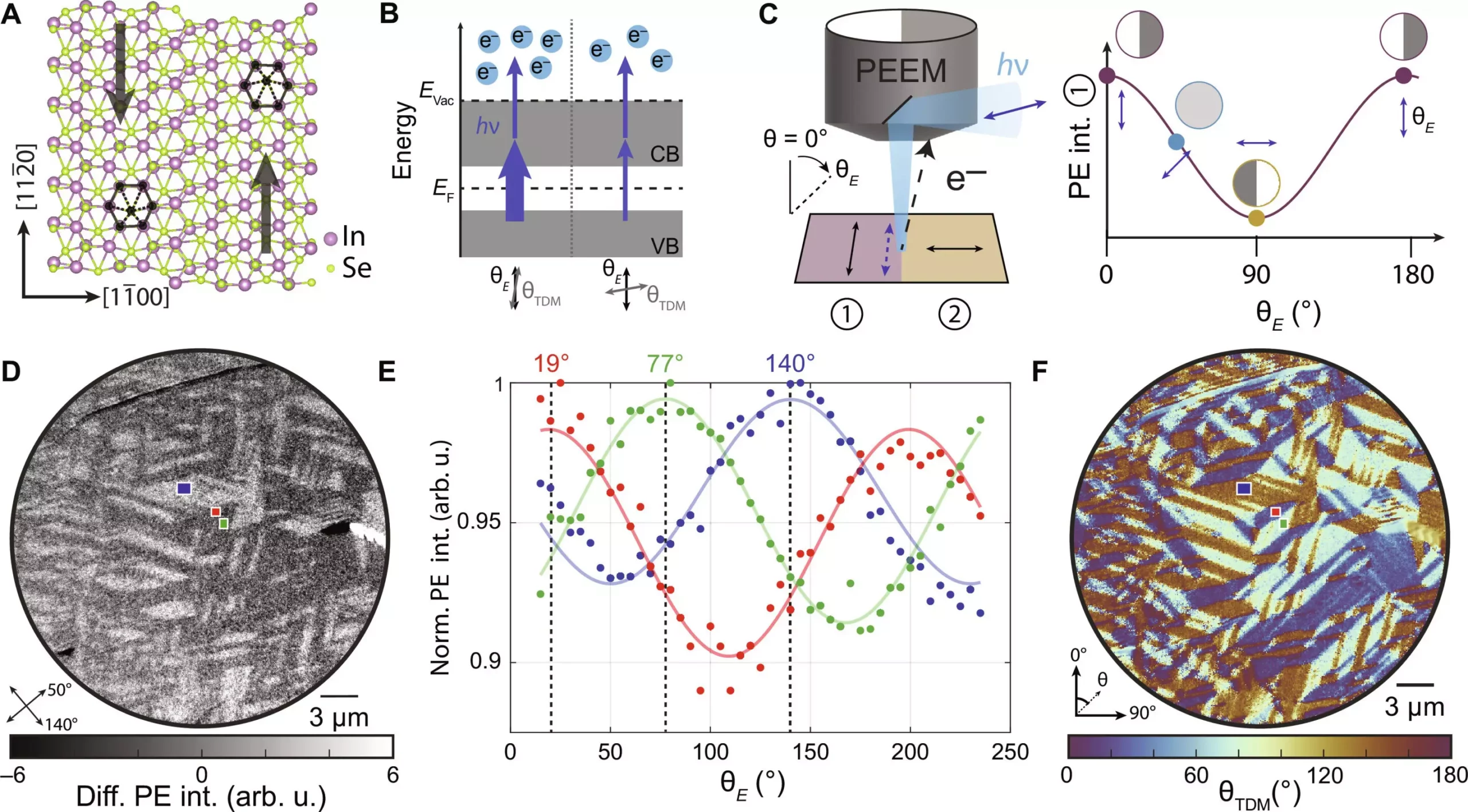
In a groundbreaking shift, King’s lab has pioneered new techniques that allow scientists to visualize antiferroelectric domains with astonishing clarity. By employing an advanced technique known as polarization-dependent photoemission electron microscopy, her team has brought forth an innovative method that combines polarized laser light with electron imaging. This fusion of techniques offers a detailed view of the electronic properties and spatial arrangements within commonly used antiferroelectric materials, such as indium selenide.
This advancement is not merely incremental; it represents a critical leap toward understanding the underlying mechanisms that control antiferroelectricity. Through this innovative approach, the researchers can map not only the orientation of dipoles but also the intricate relationships between them—information that could be pivotal in developing engineered materials with superior functionalities.
Future Prospects in Materials Science
With these new imaging techniques, King envisions a promising future where the exploration of various materials reaches unprecedented depths. The ability to visualize atomic-level interactions will enable researchers to delve into the dynamic nature of domain switching. This is particularly significant, as the switching behavior of dipoles between states can radically alter the electronic characteristics of materials.
Moreover, the inquiry into how different materials interact and establish ordered states could open new avenues for research. King’s insights into the importance of order and hierarchy in materials formation suggest that a deeper understanding of these relationships could lead to customized materials specifically tailored to industrial applications.
The study underscores a broader implication—improved imaging techniques could revolutionize not only the field of antiferroelectric materials but also materials science as a whole. By enhancing our ability to visualize and manipulate materials at the nanoscale, we can unlock the door to new technologies that are not only efficient but also essential for addressing the energy and data demands of our time.
The work being done at the University of Chicago stands as a testament to the power of innovative thinking and advanced technology in pushing the boundaries of what we know about the materials that underlie modern technology. It will not only propel antiferroelectric materials into a new realm of application but also inspire future advances in diverse facets of materials research.