Antiferromagnets, materials where adjacent atomic magnetic moments orient in opposing directions, fascinatingly exhibit zero net macroscopic magnetism. This unique characteristic positions them as strong candidates for advanced technological applications in fields like spintronics—a domain that manipulates electron spins for device technologies. The recent progress made by researchers at Harvard University, who have observed an antiferromagnetic diode effect using the material MnBi2Te4, heralds a potential breakthrough. Their findings underline the promising attributes of antiferromagnets, advocating for their inclusion in the next generation of electronics.
In a groundbreaking study published in *Nature Electronics*, the Harvard team experimentally corroborated the antiferromagnetic diode effect within even-layered MnBi2Te4, which is notable for its centrosymmetric crystal structure. This structural configuration implies a distinctive mechanism where directional charge separation is not inherent. Unlike materials traditionally employed to fabricate diodes, which exploit directional conductivity, MnBi2Te4 offers a paradigm shift in understanding how antiferromagnetic materials can serve as diodes while effectively enhancing functional device applications.
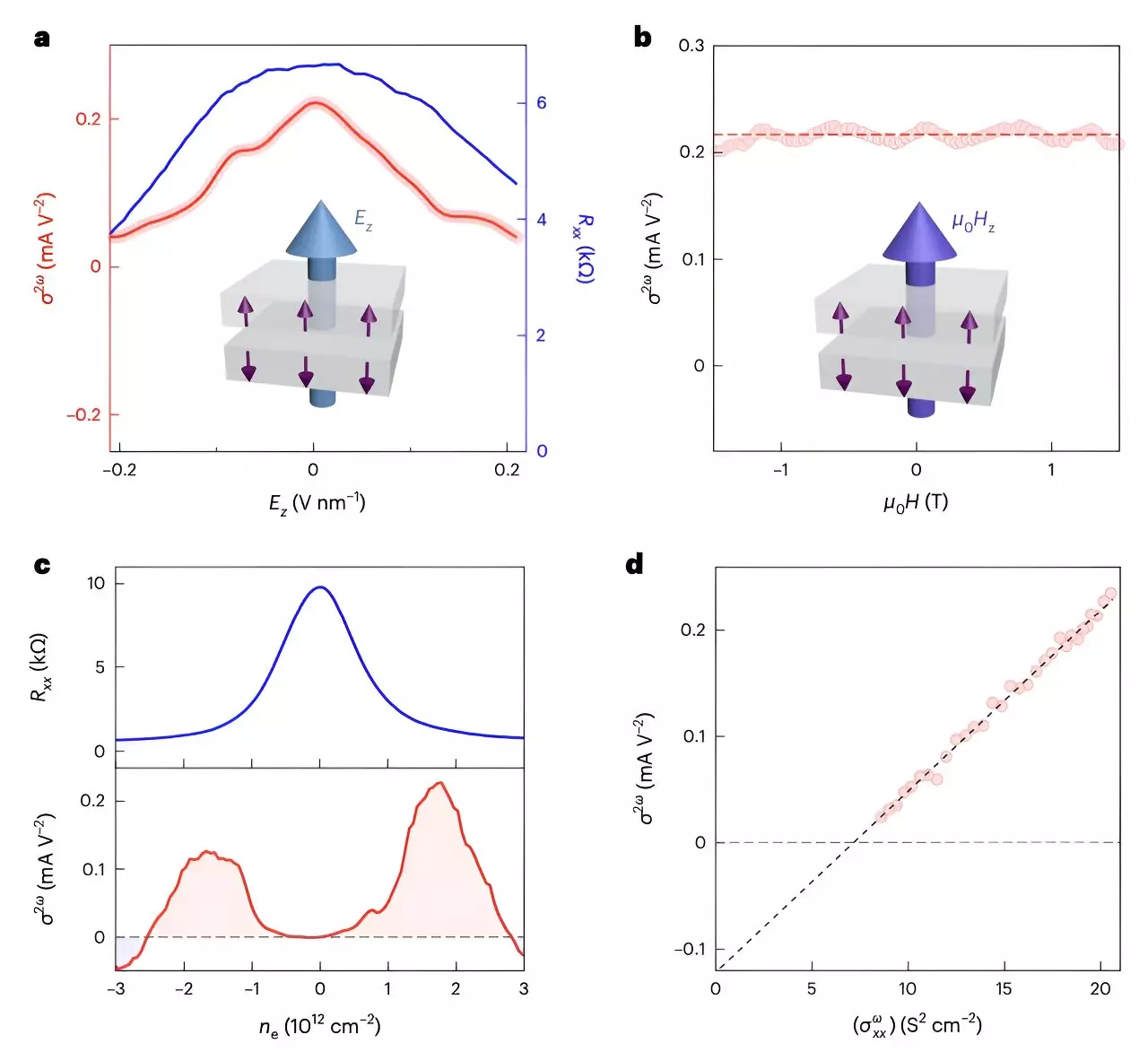
The research team, including Anyuan Gao and Shao-Wen Chen, delves deeper into the underlying mechanisms by probing various configurations. They fabricated devices with both Hall bar configurations, allowing for a direct examination of electrical characteristics, and radially distributed electrode layouts that provided comparative insights into device performance. Their observations consistently revealed the hallmark of nonlinear current transport indicative of a diode effect, prompting further investigation into the operational principles driving this innovative behavior.
Employing an array of sophisticated experimental techniques, the researchers conducted a comprehensive analysis of the antiferromagnetic properties of even-layered MnBi2Te4. Notably, spatially resolved optical methods and electrical sum-frequency generation (SFG) measurements played pivotal roles in deciphering the nonlinear characteristics of the observed electronic device. The substantial second-harmonic transport observed signifies a critical milestone in confirming the antiferromagnetic diode effect.
The combination of advanced optical techniques with electrical measurements not only highlights the multifaceted approach necessary for such complex materials, but also sets a precedent for future investigations into similar quantum materials. The outcomes underscore the adaptability of MnBi2Te4 in facilitating innovative applications, challenging conventional perspectives on material capabilities in electronic processes.
The implications of the antiferromagnetic diode effect extend beyond theoretical interest; they herald practical applications in the design of novel electronic systems. The research team asserts that this newfound effect could catalyze innovations in various technologies, including in-plane field-effect transistors, ultrafast microwave energy harvesting devices, and even high-performance antiferromagnetic logic circuits. Such advancements could noticeably elevate computing efficiency and resource management in electronic appliances, making them integral to the evolution of modern electronics.
Moreover, the discovery fosters a broader inquiry into the intersection of antiferromagnetism and superconductivity. The team alludes to prior observations of superconducting diode effects in non-centrosymmetric materials, encouraging further explorations into how these phenomena can intertwine to create even more effective electronic systems. This line of inquiry is particularly promising, as it not only maintains focus on improving current technology but also on pushing the frontiers of quantum computing and communications.
As the study at Harvard highlights, the antiferromagnetic diode effect contains immense potential to reform electronic applications appreciably. The researcher’s innovative methodologies and thorough investigative approaches showcase the intricate relationship between material properties and electronic functionalities. Moving forward, this work lays the groundwork for expansive examination into antiferromagnetic materials, increasing their feasibility in practical applications and inciting a new era where quantum materials play a central role in tomorrow’s technological landscape. The fusion of fundamental research with practical application such as this exemplifies the dynamic evolution of materials science, setting a compelling stage for future breakthroughs.